DFN

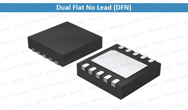
Dual Flat No Lead (DFN)
Because dual flat no-lead package has no leads and has shorter bond wire lengths, it provides a higher electrical performance than leaded packages due to less inductance.
Available package ranges from 2.0×1.5mm to 9.0×9.0mm in size. The dimensional tolerance and positioning accuracy affects subsequent processes as the package size shrinks and the lead count increases. In subsequent processes, the PCB layout and stencil designs are critical to ensure sufficient solder coverage between the package and the printed circuit board (PCB). When designing the PCB layout, refer to the case outline drawing to obtain the package dimensions and tolerances.
DFN package usually have pad counts that range from 3 to 32. The typical size body size has a length that ranges from 2mm to 9mm. The pad pitch (distance between pads) typically ranges from 0.4mm or 0.95mm. A thinner version exists and is known as the TDFN.
| Properties of Some Examples | ||||
| Part Number | No. of Pins | Body Size | Body Thickness | Pad Pitch |
| DFN-6 | 6 | 3 x 3 mm | 0.9 mm | 0.95 mm |
| DFN-8 | 8 | 2 x 3 mm | 0.9 mm | 0.50 mm |
| DFN-10 | 10 | 4 x 4 mm | 0.9 mm | 0.65 mm |
| DFN-16 | 16 | 1.6 x 4 mm | 0.80 mm | 0.50 mm |
